What is Green Energy?
Green energy is a form of renewable energy that has minimal environmental impact during production. Unlike fossil fuels such as coal and natural gas, green energy generates electricity without emitting greenhouse gases, helping to mitigate climate change and promote sustainable development. Common sources of green energy include solar photovoltaic (PV) energy, wind energy, geothermal energy, biogas, eligible forms of biomass, and low-impact hydropower.
Among these, solar PV plays a critical role. It harnesses energy directly from the sun, providing a clean, renewable source of electricity with a relatively low carbon footprint and minimal environmental impact.
Globally, solar energy deployment over the past six years is now avoiding around 1.4 gigatonnes (Gt) of annual carbon emissions, compared to approximately 900 million tonnes (Mt) from wind power, 190 Mt from nuclear energy, and 80 Mt and 65 Mt from electric vehicles and heat pumps, respectively (Global Energy Review by IEA, 2025).

Figure 1
Source : Global Energy Review, IEA
Why Solar Energy Is Called the Energy of the Future
Historically, the high upfront cost of solar installations was a major barrier for many users. However, recent advancements in solar technology—especially in panel design and manufacturing—have significantly driven down costs and made solar energy more accessible to a broader range of users.
Key innovations have driven the transformation of solar panel technology. The main technologies today include TOPCon, HJT, perovskite, and BC. TOPCon (Tunnel Oxide Passivated Contact) technology further improves efficiency by minimizing energy loss and performing well under low-light conditions, offering higher energy yields. HJT (Heterojunction Technology) combines crystalline silicon with thin-film technology for high efficiency and durability. Though more expensive, HJT panels provide long-term energy savings due to their superior performance and lifespan. PSC (Perovskite Solar Cell) technology is based on the use of perovskite materials, primarily in the light-absorbing layers of the cell. It has the potential to create solar panels that can be easily deposited onto various surfaces, including flexible and textured ones, which are cheap to produce and potentially more efficient than traditional silicon-based cells. BC (Back Contact) technology refers to solar panels in which all the electrical contacts—both positive and negative—are located on the rear side of the solar cell. This contrasts with most conventional technologies, where metallic contacts on the front side partially shade the light-absorbing surface.
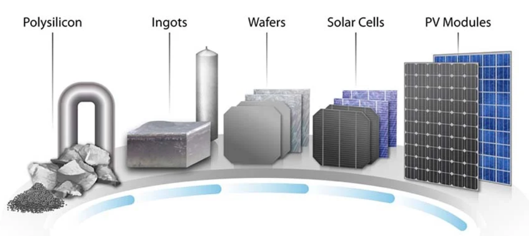
Figure 2
Source : Solar Technology Cost Analysis, NREL
As a result, solar PV costs have dropped by 90% over the past decade, transforming solar energy to the most affordable electricity sources in many countries over the past 40 years (Ritchie, 2024). Looking ahead, solar energy is expected to become the world's largest green energy source by 2029, having already accounted for 81% of all new renewable capacity added globally in 2024 (Hemetsberger, Dunlop and Schmela, 2025). A ture future energy for us all.
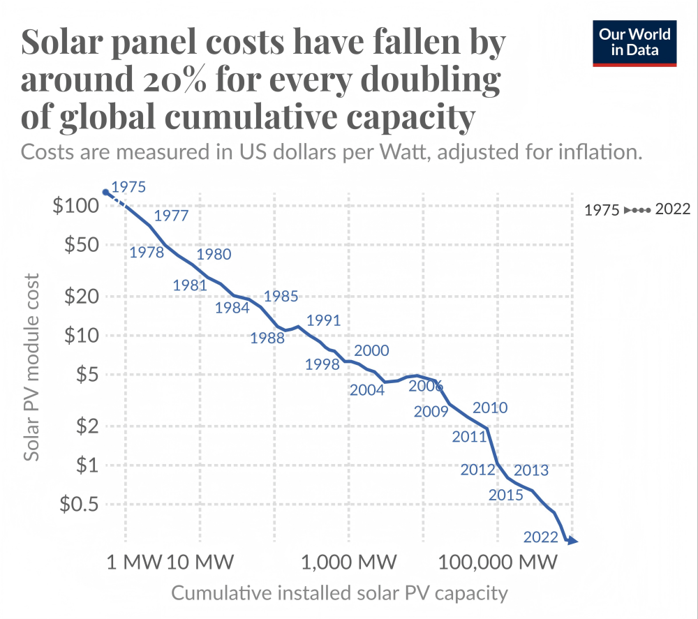
Figure 3
Source : IRENA (2023); Nemet (2009); Farmer and Lafond (2016).
Solar Wafer: How Wafer Technologies Enhance Solar PV
A solar wafer is a thin slice of silicon cut from a larger ingot and serves as the foundation of a solar cell. As a key component in the PV supply chain, advancements in wafer technology have greatly improved both efficiency and cost-effectiveness.
Increasing Wafer Size
A larger surface area means more space to collect sunlight. Over the past 40 years, wafer sizes have grown significantly. From 1981 to 2013, sizes gradually increased from 100 mm and 125 mm to larger formats, including 156.75 mm, 157.3 mm, and 166 mm. As the industry moved toward large-size solar panels, the G12 wafer (210 mm) was introduced in 2019. Following this trend, 182 mm became the mainstream size in 2023, and 210 mm already became dominant by 2025.
Reducing Wafer Thickness
Since silicon remains a major cost in solar wafer production, reducing wafer thickness is key to lowering costs and increasing output. In 2000, wafers were 300–400μm thick, resulting in significant material waste. By 2010, the thickness dropped to 150–180μm. Since then, thinning has accelerated, with modern wafers as thin as 110 μm—and in some cases, even 80μm.
Optimizations of Key Qualifications
In addition, reducing oxygen concentration, improving minority carrier lifetime, and enhancing resistivity concentration all contribute directly to increasing the photoelectric conversion efficiency of solar cells. These improvements drive greater efficiency across the entire PV value chain.

The Pioneer of Solar Wafer
At QJSOLAR, we are working toward a future where green energy is accessible, reliable, and sustainable. As pioneer in China solar monocrystalline field, QJSOLAR has over 20 years of experience in N-type production and has pioneered several key technologies.
Currently, QJSOLAR is building a planned total production capacity of 20 GW for solar wafers and 40 GW for solar ingots in Yunnan, China. Our goal is to ensure every wafer delivers high quality and performance, helping solar energy operate efficiently and contributing to a greener, more sustainable planet.
Renewable
Farmer, J. D., & Lafond, F. (2016). How predictable is technological progress? Research Policy, 45(3), 647–665. https://doi.org/10.1016/j.respol.2015.11.001
Federal Tax Credits for Solar Manufacturers. (n.d.). Energy.gov. https://www.energy.gov/eere/solar/federal-tax-credits-solar-manufacturers
Global Market Outlook for Solar Power 2025-2029 - SolarPower Europe. (2025). Solarpowereurope.org. https://www.solarpowereurope.org/insights/outlooks/global-market-outlook-for-solar-power-2025-2029/detail
IEA. (2025, March 24). Global Energy Review 2025 – Analysis - IEA. IEA. https://www.iea.org/reports/global-energy-review-2025
IRENA. (2023). Renewable Power Generation Costs in 2022. Www.irena.org. https://www.irena.org/Publications/2023/Aug/Renewable-Power-Generation-Costs-in-2022
Performance Curve Database. (n.d.). Pcdb.santafe.edu. https://pcdb.santafe.edu/graph.php?curve=158
Ritchie, H. (2024, June 13). Solar Panel Prices Have Fallen by around 20% Every Time Global Capacity Doubled. Our World in Data. https://ourworldindata.org/data-insights/solar-panel-prices-have-fallen-by-around-20-every-time-global-capacity-doubled
US Department of Energy. (2022). Solar Photovoltaic Cell Basics. Energy.gov. https://www.energy.gov/eere/solar/solar-photovoltaic-cell-basics
US EPA, O. (n.d.). What Is Green Power? [online] 19january2017snapshot.epa.gov. Available at: https://19january2017snapshot.epa.gov/greenpower/what-green-power_.html.
Wikipedia Contributors. (2019, March 29). Silicon. Wikipedia; Wikimedia Foundation. https://en.wikipedia.org/wiki/Silicon
Wikipedia Contributors. (2019, October 10). Oxygen concentrator. Wikipedia; Wikimedia Foundation. https://en.wikipedia.org/wiki/Oxygen_concentrator
Wikipedia Contributors. (2025, May 23). Carrier lifetime. Wikipedia; Wikimedia Foundation.
Wikipedia. (2019, March 7). Electrical resistivity and conductivity. Wikipedia; Wikimedia Foundation. https://en.wikipedia.org/wiki/Electrical_resistivity_and_conductivity


 IngotsLearn More





 Please Click On The Question You Want To Consult