SNEC 2025, the world's most influential and large-scale international photovoltaic (PV) event, officially opened on June 11, 2025, in Shanghai. Renowned for its global reach and professional focus, the exhibition showcases a comprehensive array of innovations spanning PV manufacturing equipment, materials, solar cells, application products, modules, and more. The event also features in-depth discussions on the future of PV and energy storage markets, collaborative development trends, industrial policies, and cutting-edge technologies. PV industry leaders from around the globe have gathered to chart a bold vision for clean energy development and to inject fresh momentum into the global energy transition.
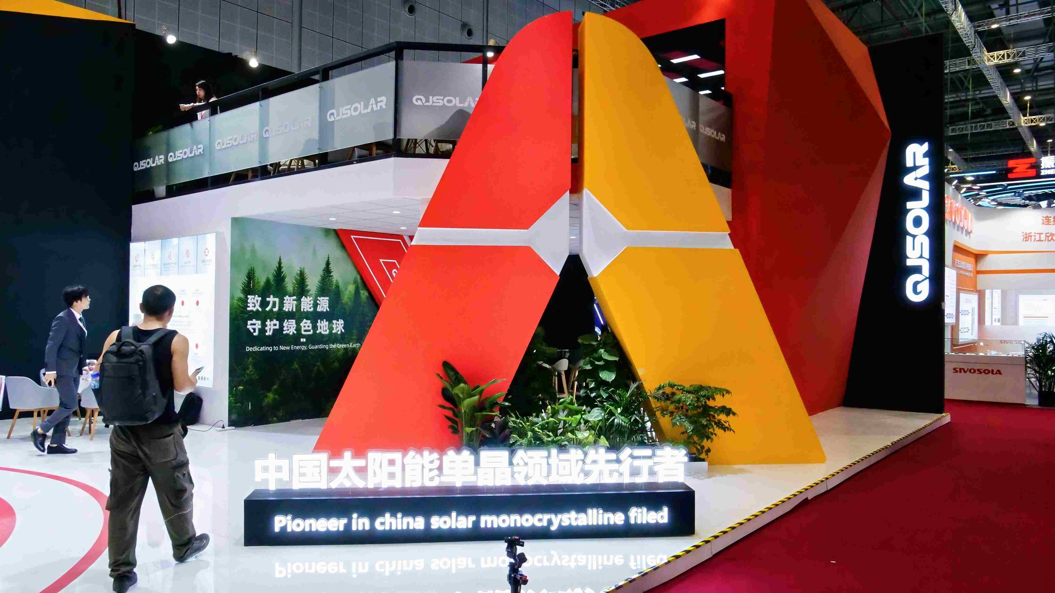
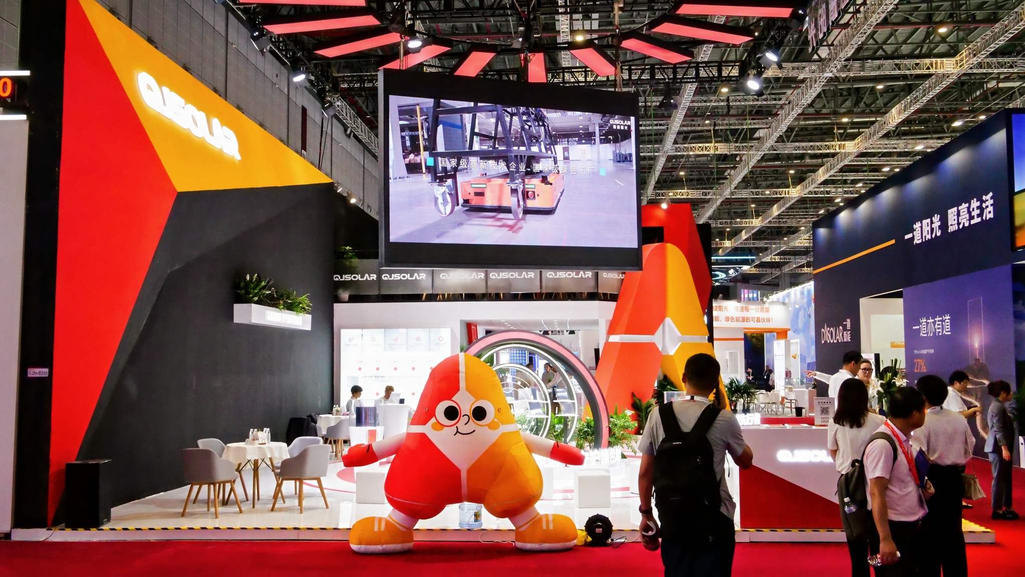
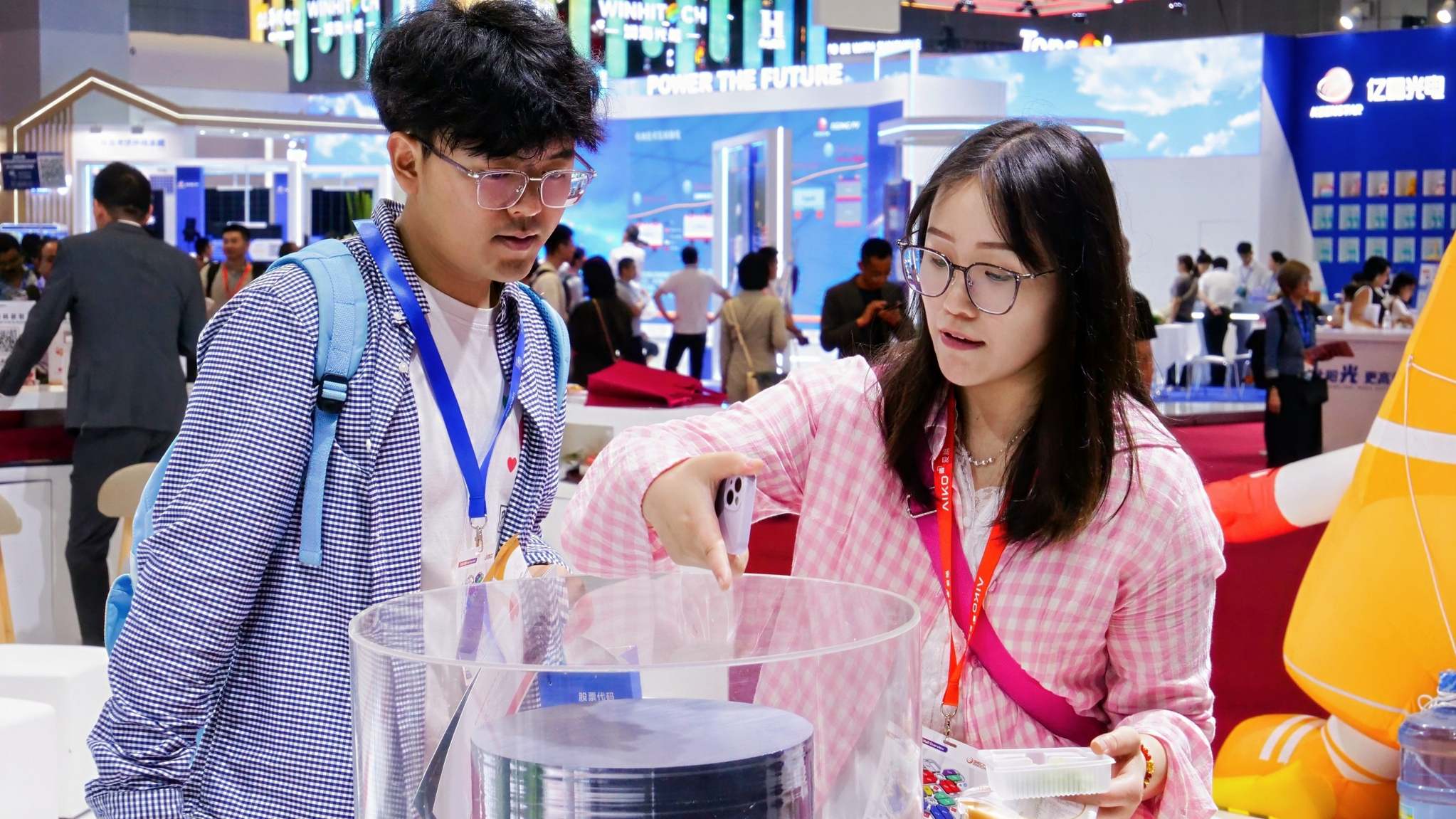
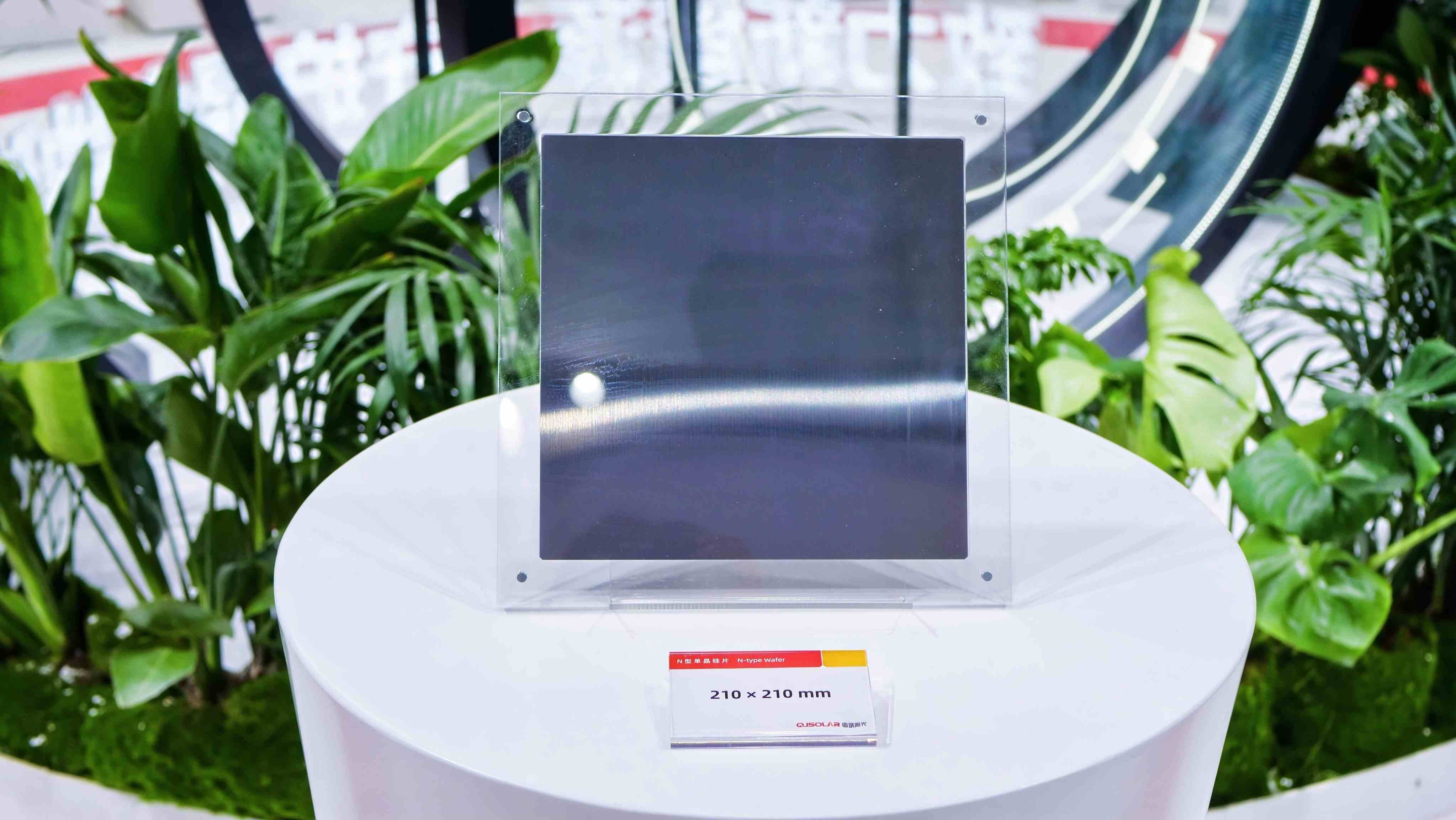
As pioneer in China's solar monocrystalline field, QJSOLAR drew considerable attention on the first day of the exhibition with its uniquely designed booth and immersive displays. With over 20 years of experience in N-type production, the company presented its high-quality silicon wafers and ingots, offering a comprehensive view of its technological evolution and core strengths. With a steadfast commitment to supporting downstream solar cell manufacturing, QJSOLAR continues to make significant contributions to the robust growth of the PV value chain.
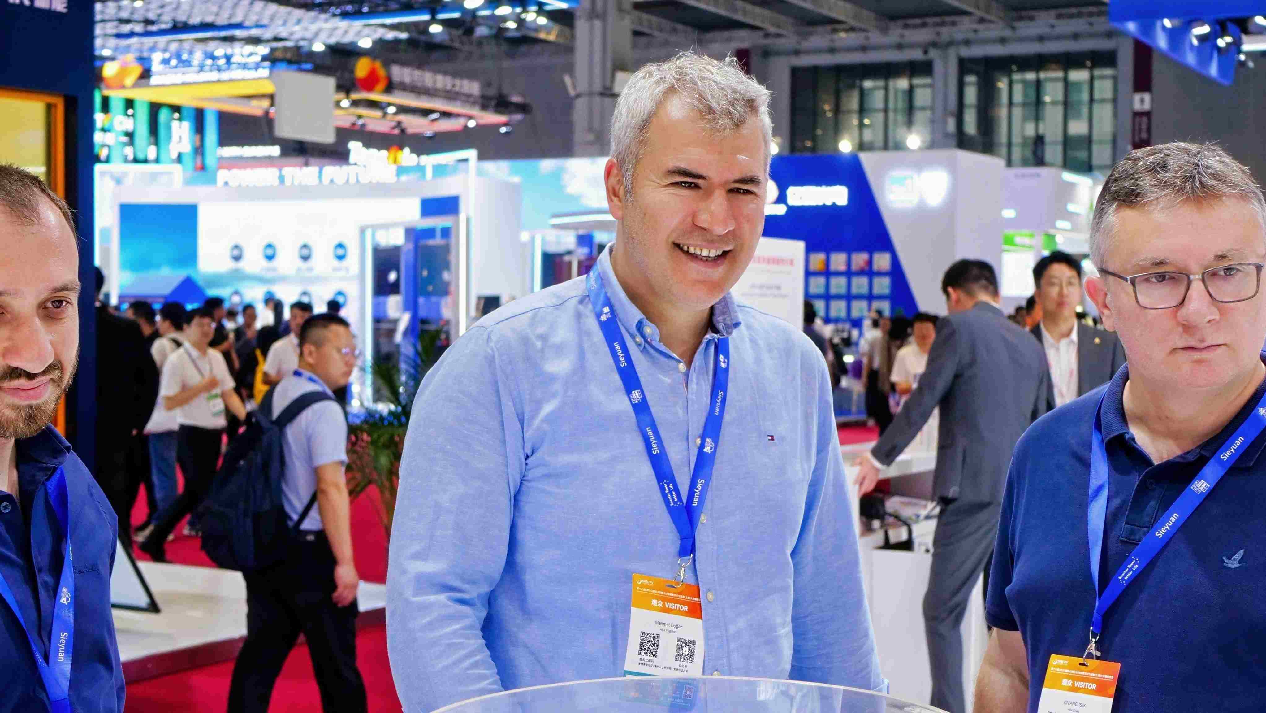
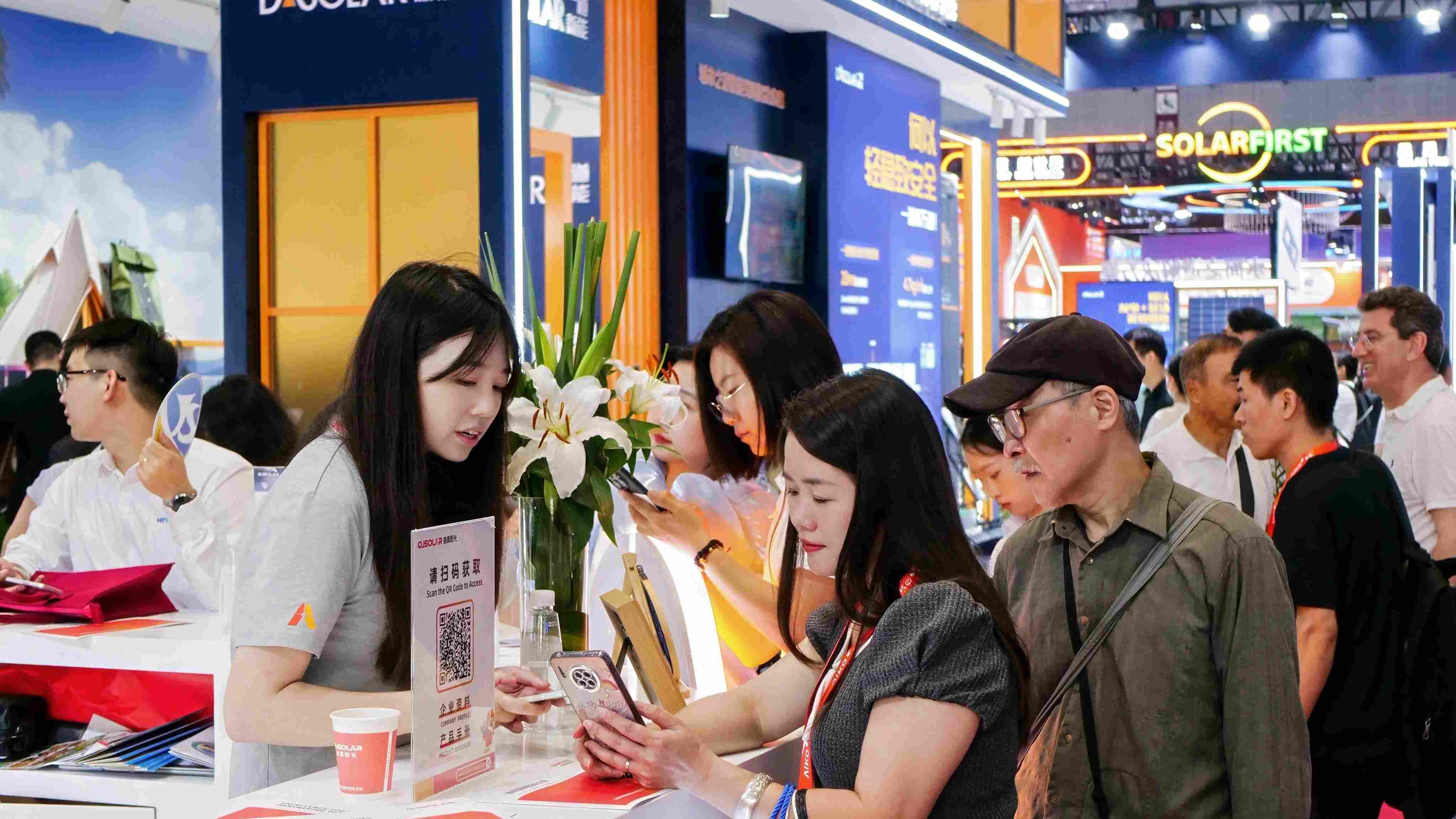
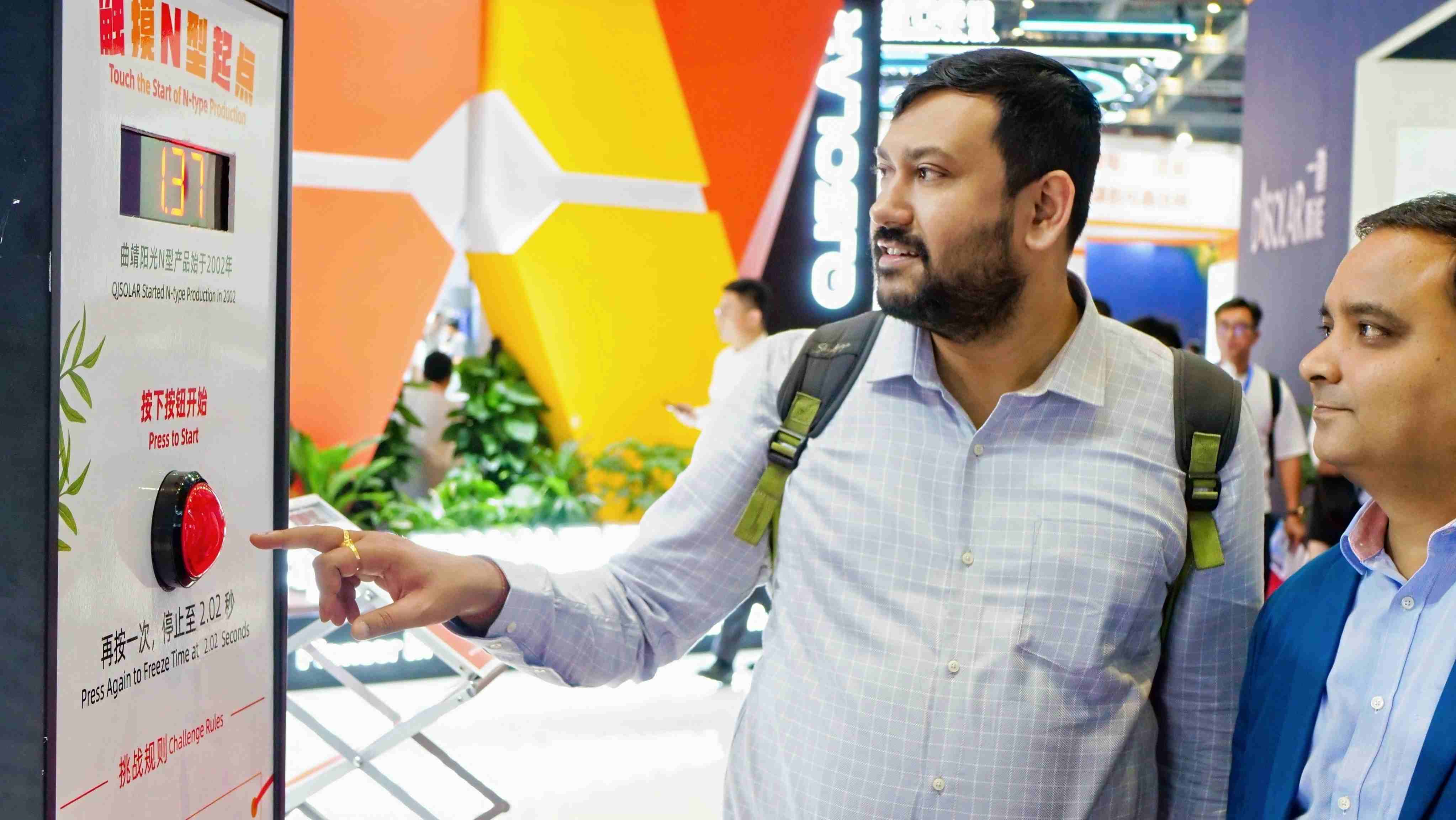
At the exhibition, QJSOLAR placed a strong spotlight on its large-format, high-purity N-type silicon wafers. Having initiated N-type product R&D and mass production as early as 2002, the company now boasts more than two decades of expertise and is a pioneer in several key technologies. With ongoing advancements in both wafer and ingot quality, QJSOLAR remains dedicated to driving excellence across the board. The company's smart factory, featuring fully integrated digital and intelligent systems, ensures complete traceability throughout the entire production process. Equipped with state-of-the-art machinery, the factory aims to set a new benchmark in "advanced capacity" within the PV industry, consistently enhancing the efficiency of downstream solar cells and delivering tangible value across the entire supply chain.


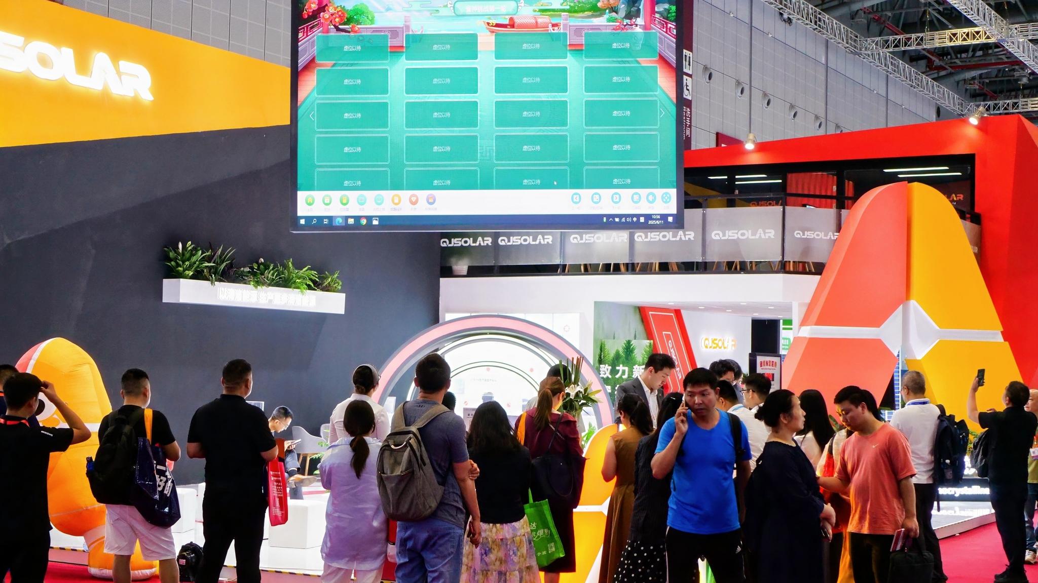
On the morning of June 11, QJSOLAR's booth was filled as the company hosted a technical presentation titled “Technological Challenges for Monocrystalline Silicon in Current Market Conditions.”Chen Lifang, Chief Engineer of Manufacturing Technology at QJSOLAR's Intelligent Manufacturing Center, delivered an in-depth analysis of the technological bottlenecks currently facing monocrystalline silicon production. Against the backdrop of surging market demand and intensifying industry competition, she outlined QJSOLAR’s targeted solutions: utilizing ultra-pure silicon raw materials and graphite thermal field components to enhance minority carrier lifetime; optimizing solidification rates and doping processes to improve wafer resistivity uniformity; continuously refining thermal field design and crystal pulling techniques to reduce interstitial oxygen content; and advancing intelligent manufacturing to boost efficiency and reduce production costs.
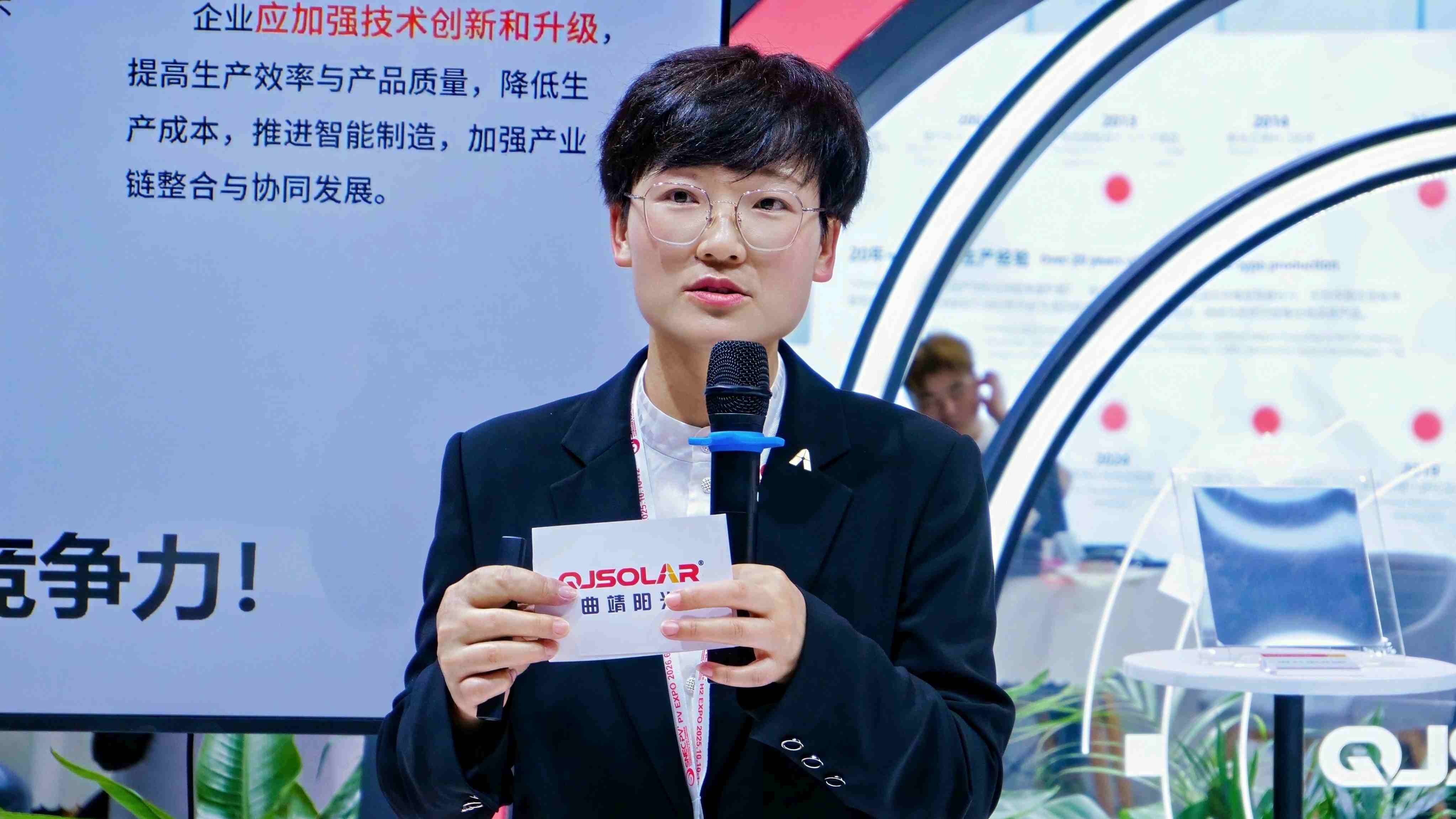
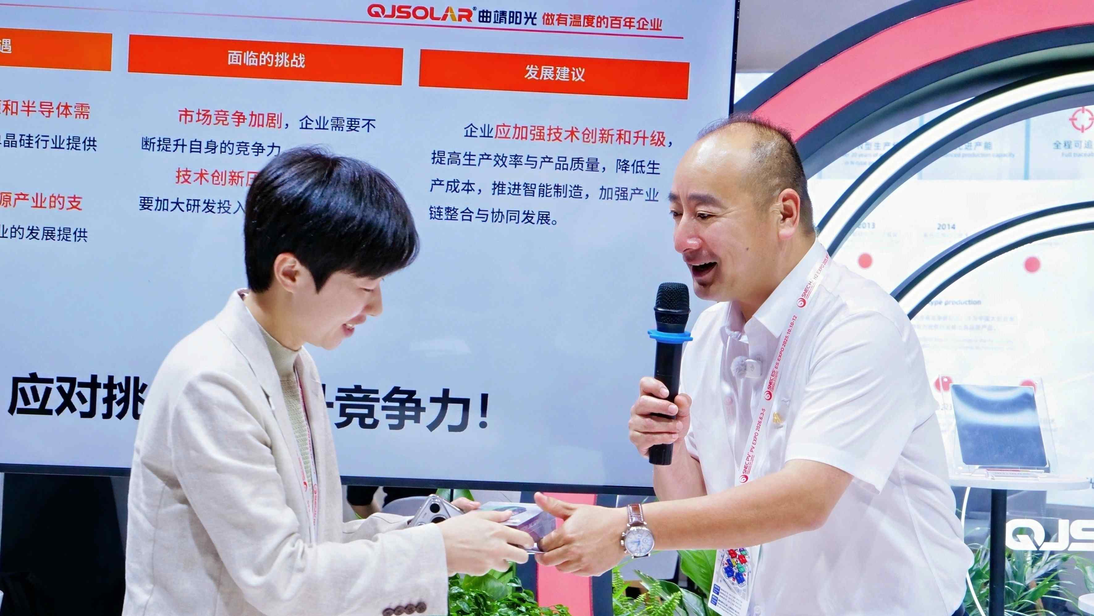
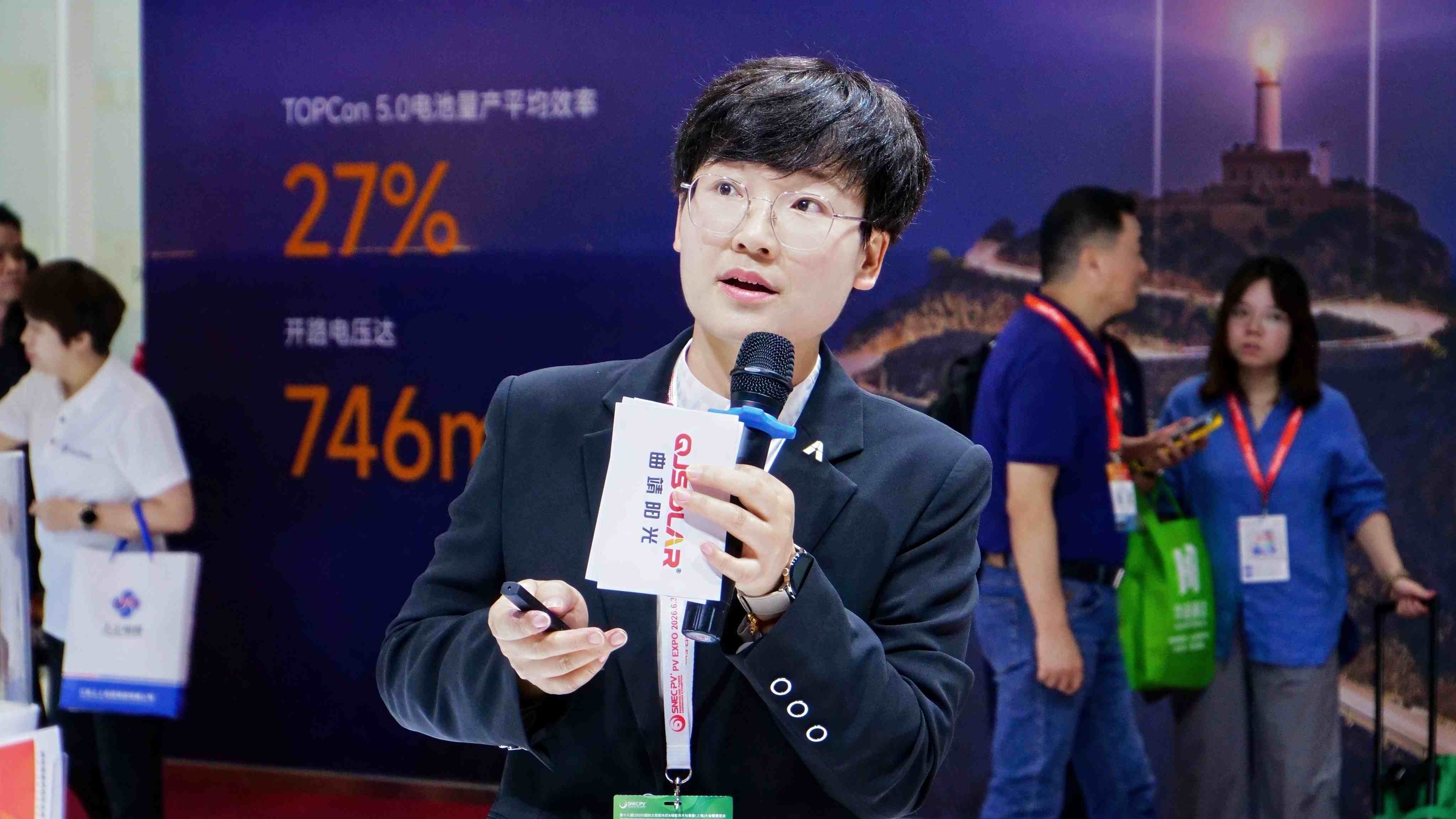
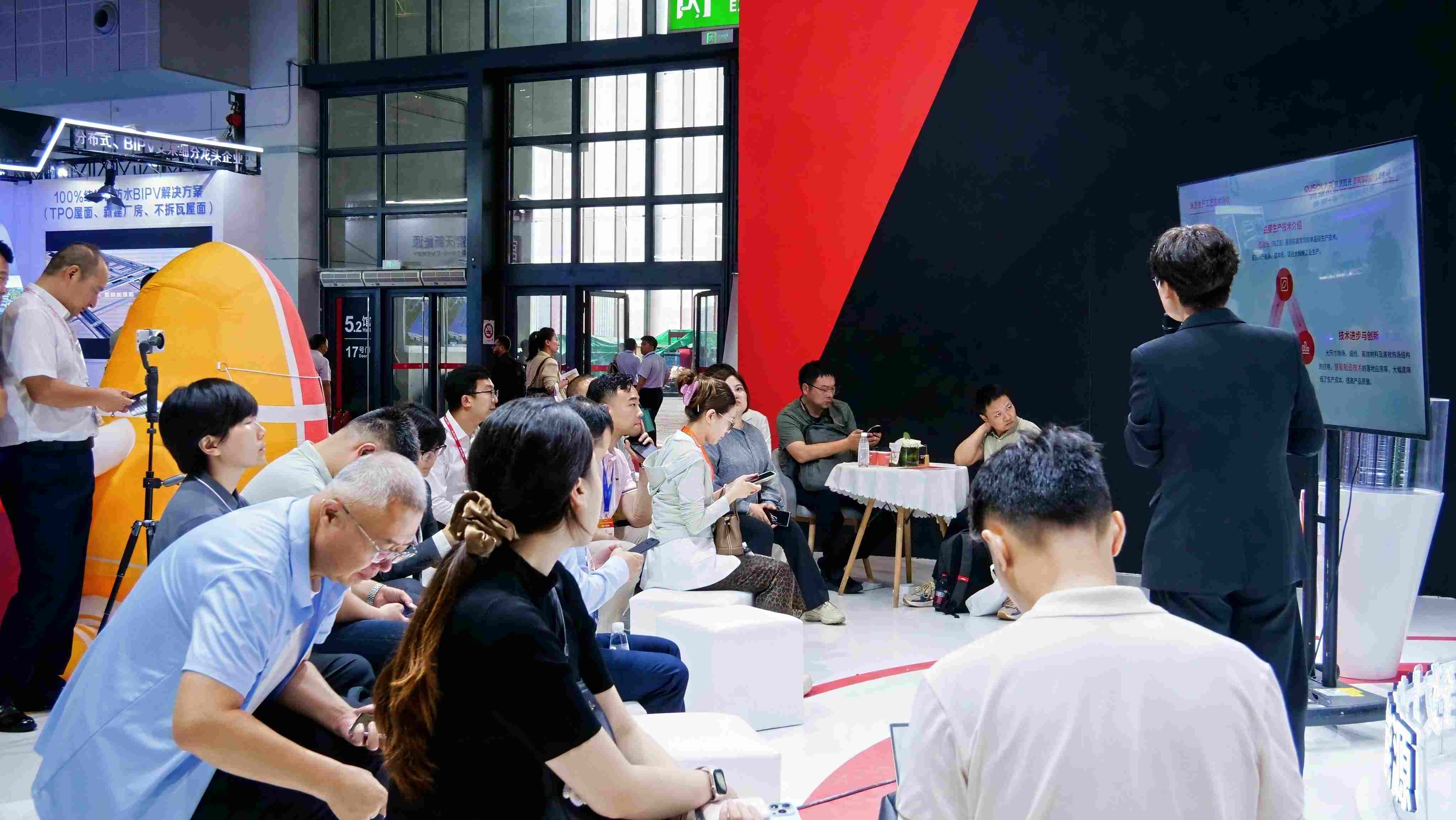
The presentation showcased not only QJSOLAR's technical strength and forward-looking approach but also offered practical insights for improving cost-efficiency across the PV sector. Through this exchange, the company engaged in deeper, multidimensional dialogue with industry partners and visitors, contributing to the upgrade and development of the solar value chain. Together, they are working to accelerate the global adoption of clean energy and contribute meaningfully to a sustainable future for humanity.


 IngotsLearn More





 Please Click On The Question You Want To Consult